-


 Restoring damaged solder pads? Help?
I know this is a big question but even links would be great. This is the last thing I need to finish my first saber and I would hate to waste a soundboard over a solder pad. I know how to prevent this from happening now but could really use the help and it would be a great addition to the forum.
I managed to do some great soldering on my first attempt till I needed to redo some, and by that point my soldering iron was acting up.
So...I think I burned up a pad from not tinning my tip properly. The heat wasn't transferring and I held the tip to my board a little too long.
For example...My US 2.5
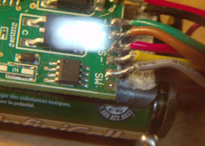
- On one pad (accent LED) it was blackened but had a small spot of solder the size of the hole in the pad and it took ok and seems fine.
- I was able to attach to the other pad (activation switch negative) but it seems to make no connection and is quite blackened.
My Question is how can one clean burnt/damaged pads and what options are there for repairing/replacing or bypassing?
Any help would be greatly appreciated. I will be too happy to post a detailed a build log when all is done...
-
Jedi Council Member


Can you post pics?
pics (in this situation at least) are crucial..so we can see where the pads is.. if ther is an alternate route/pad for the same thing..or maybe another place you can solder..like to the trace from that pad or something..
also getting 'black' might not be 'as' bad' as you thin kit is.. it could be the solder mask getting burnt as well..
Im not sure what can be used to clean it? rubbibg alcohol/q-tip perhaps?? at least to see what the real damage is like and what your ultimately left with to use.
-
-
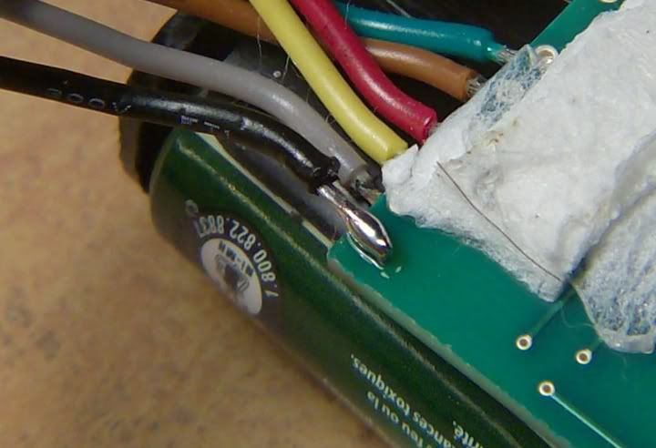
The one pad that's giving me trouble now is the switch pad on the outside, the corner of the board. I have to detach the wire on there now to show underneath, take a pic, and set-up a photobucket account...I'll do that early tommorrow.
The wire currently appears fine (nice looking solder) but since I saw under it before a feeble attempt to solder I can tell it's not getting a connection.
Oh yeah! The other side of the board looks like a great idea. It is connected to the battery case wtih mounting tape. I just hope I don't do more damage trying to fix this...oh my. Glad I waited to glue gun the wires to the battery pack until my final cram. Once I get through all this my next build should be a breeze in comparison.
Cleaning of burnt rosin would be the best case senario...hope you're right. thx
Last edited by Crystal Chambers; 12-22-2009 at 11:51 AM.
-
-
Jedi Council Member
couple suggestions..
1.) I would always make my 'leads/wires' have as 'little' needed exposed wires showing.. so that when you solder the wires to the board.. there is a bunch of exposed wire moving around.possibly grounding on anythign else on the board/hilt...etc.
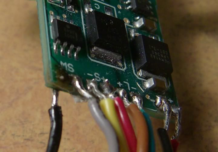
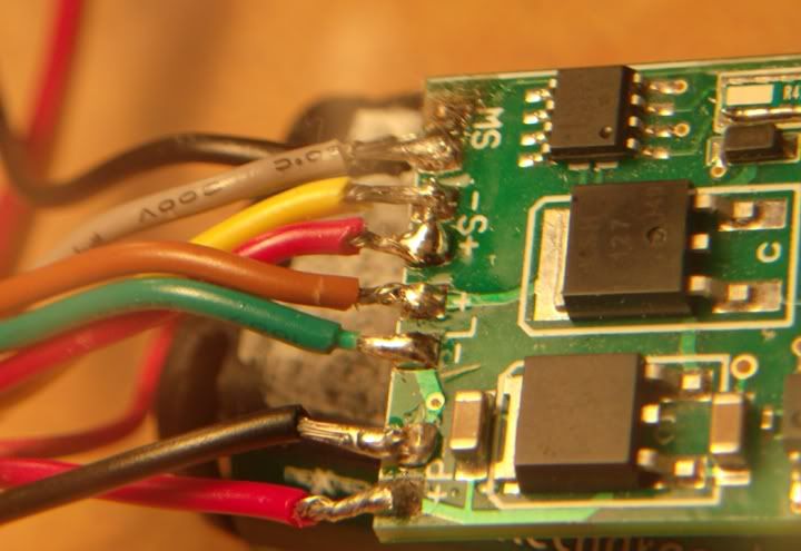
2.) hmm.. Im looking at an extras US 2.5 I have laying around.. all my wires are soldered to the UNDERSIDE of the board..none on the top pads (all done on the underside on the through holes)
are there any solder drop/spatter anywhere? creating a ground or connection? (bridge)
to anything?
what switch are you using? are you trying to use/wire in a re-charge port?
-
I did have shorter length exposed but it melted when I tinned the wires. I had it covered in film cases and made sure no wires would short no bridges..etc.
It's a momentary switch and yes recharge port. I followed a diagram here that everyone said worked it was very clear.
I should mention again that all was working fine until the wire came loose and then wouldn't work when I tried to re-attach it.
Last edited by Crystal Chambers; 12-23-2009 at 08:02 AM.
-
Jedi Council Member
well..in 'my' opinion..
solering to the bottom through hole isnt going top help much AT ALL..
and heres why I say that.. you ripped the pad off.. meing there is NO trace left connection the placted through hole you soldered to.
if you look on the TOP of the board..you will see a very (very) thin trace going up the whole side of the board..toward the PIC18 chip...
THIS is the line you need to tap into.
I would try to see if you can scrap (VERY, VERY , VERY lightly) the top solder mask off that trace on the top side of the board.. and either run some solder to the wher to through hole is.. or try and re-solder to the top.
but it solder is SOLID on the bottom where you put the wire.. try to just scrap off a bit of the solder mask..to revela the trace under it..then solder form the trace to the pad again..making sue enough get in the HOLE to make contact with the wire on the bottom.
-
It does appear to be a solid connection on the underside. I believe I see the trace...the green line running stright down the board and then curves towards the W of the SW. The only other obstacle I can see is trying to get the burnt up surface off to make a connection throught the hole. Purhaps if I use a small drill bit and twist it by hand on the spot to expose the solder underneath through the hole. Does this seem like a good idea?
Also if I scape the surface of the trace to reveal the connection what should I use? And what do I look for to know that I'm doing it, or have done it correctly?
-
 Posting Permissions
- You may not post new threads
- You may not post replies
- You may not post attachments
- You may not edit your posts
-
Forum Rules


 Reply With Quote


Bookmarks